- 您现在的位置:买卖IC网 > Sheet目录327 > HW-SPAR3A-SK-UNI-G (Xilinx Inc)KIT STARTER W/SPARTAN-3A
R
Analog-to-Digital Converter (ADC)
The amplifier interface is relatively slow, supporting only about a 10 MHz clock frequency.
UCF Location Constraints
including the I/O pin assignment and I/O standard used.
NET
NET
NET
NET
"SPI_MOSI"
"AMP_CS"
"SPI_SCK"
"AMP_SHDN"
LOC
LOC
LOC
LOC
=
=
=
=
"AB14"|
"W6" |
"AA20"|
"W15" |
IOSTANDARD
IOSTANDARD
IOSTANDARD
IOSTANDARD
=
=
=
=
LVTTL
LVTTL
LVTTL
LVTTL
|
|
|
|
SLEW
SLEW
SLEW
SLEW
=
=
=
=
SLOW
SLOW
SLOW
SLOW
|
|
|
|
DRIVE
DRIVE
DRIVE
DRIVE
=
=
=
=
8 ;
4 ;
12 ;
4 ;
NET
"AMP_DOUT"
LOC
=
"T7" |
IOSTANDARD
=
LVTTL
;
Figure 10-5:
UCF Location Constraints for the Pre-amplifier Interface (AMP)
Analog-to-Digital Converter (ADC)
The LTC1407A-1 provides two ADCs. Both analog inputs are sampled simultaneously
when the AD_CONV signal is applied.
Interface
is shared with other devices on the SPI bus. The active-High AD_CONV signal is the
active-Low slave select input to the DAC. The DAC_CLR signal is the active-Low,
asynchronous reset input to the DAC.
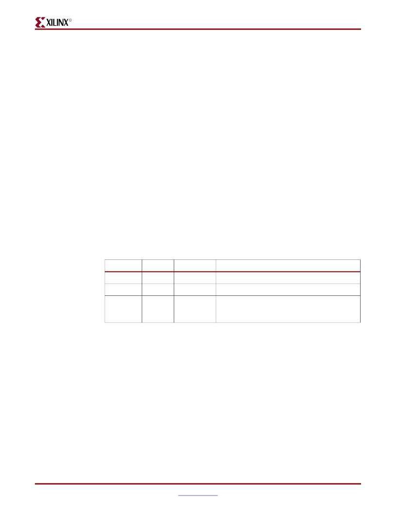
Table 10-3:
ADC Interface Signals
Signal
FPGA Pin
Direction
Description
SPI_SCK
AD_CONV
ADC_OUT
AA20
Y6
D16
FPGA ADC Clock
FPGA ADC Active-High, initiates conversion process.
FPGA ADC Serial data. Presents the digital representation of the
sample analog values as two 14-bit two’s
complement binary values.
SPI Control Interface
When the AD_CONV signal goes High, the ADC simultaneously samples both analog
channels. The results of this conversion are not presented until the next time AD_CONV is
asserted, a latency of one sample. The maximum sample rate is approximately 1.5 MHz.
The ADC presents the digital representation of the sampled analog values as a 14-bit, two’s
complement binary value.
Spartan-3A FPGA Starter Kit Board User Guide
UG330 (v1.3) June 21, 2007
81
发布紧急采购,3分钟左右您将得到回复。
相关PDF资料
HW-SPAR3AN-SK-UNI-G
KIT STARTER SPARTAN-3 AN
HW-V4-ML403-UNI-G-J
EVALUATION PLATFORM VIRTEX-4
HW-V4-ML405-UNI-G-J
EVALUATION PLATFORM VIRTEX-4
HW-V4-ML410-UNI-G-J
EVALUATION PLATFORM VIRTEX-4
HW-V5-ML501-UNI-G
EVALUATION PLATFORM VIRTEX-5
HW-V5-ML507-UNI-G
EVAL PLATFORM V5 FXT
HW-V5-ML550-UNI-G
EVALUATION PLATFORM VIRTEX-5
HW-V5-ML555-G
BOARD EVAL FOR VIRTEX-5 ML555
相关代理商/技术参数
HW-SPAR3A-SK-UNI-G-J
功能描述:KIT STARTER W/SPARTAN-3A RoHS:是 类别:编程器,开发系统 >> 通用嵌入式开发板和套件(MCU、DSP、FPGA、CPLD等) 系列:Spartan®-3A 产品培训模块:Blackfin® Processor Core Architecture Overview
Blackfin® Device Drivers
Blackfin® Optimizations for Performance and Power Consumption
Blackfin® System Services 特色产品:Blackfin? BF50x Series Processors 标准包装:1 系列:Blackfin® 类型:DSP 适用于相关产品:ADSP-BF548 所含物品:板,软件,4x4 键盘,光学拨轮,QVGA 触摸屏 LCD 和 40G 硬盘 配用:ADZS-BFBLUET-EZEXT-ND - EZ-EXTENDER DAUGHTERBOARDADZS-BFLLCD-EZEXT-ND - BOARD EXT LANDSCAP LCD INTERFACE 相关产品:ADSP-BF542BBCZ-4A-ND - IC DSP 16BIT 400MHZ 400CSBGAADSP-BF544MBBCZ-5M-ND - IC DSP 16BIT 533MHZ MDDR 400CBGAADSP-BF542MBBCZ-5M-ND - IC DSP 16BIT 533MHZ MDDR 400CBGAADSP-BF542KBCZ-6A-ND - IC DSP 16BIT 600MHZ 400CSBGAADSP-BF547MBBCZ-5M-ND - IC DSP 16BIT 533MHZ MDDR 400CBGAADSP-BF548BBCZ-5A-ND - IC DSP 16BIT 533MHZ 400CSBGAADSP-BF547BBCZ-5A-ND - IC DSP 16BIT 533MHZ 400CSBGAADSP-BF544BBCZ-5A-ND - IC DSP 16BIT 533MHZ 400CSBGAADSP-BF542BBCZ-5A-ND - IC DSP 16BIT 533MHZ 400CSBGA
HW-SPAR3-CPLD-DK
功能描述:STARTER KIT BUNDLE SPARTAN3/CPLD RoHS:否 类别:编程器,开发系统 >> 过时/停产零件编号 系列:- 标准包装:1 系列:- 传感器类型:CMOS 成像,彩色(RGB) 传感范围:WVGA 接口:I²C 灵敏度:60 fps 电源电压:5.7 V ~ 6.3 V 嵌入式:否 已供物品:成像器板 已用 IC / 零件:KAC-00401 相关产品:4H2099-ND - SENSOR IMAGE WVGA COLOR 48-PQFP4H2094-ND - SENSOR IMAGE WVGA MONO 48-PQFP
HW-SPAR3-CPLD-DK-J
功能描述:KIT HDWR FOR SPARTAN3/CPLD-JAPAN RoHS:否 类别:编程器,开发系统 >> 过时/停产零件编号 系列:- 标准包装:1 系列:- 传感器类型:CMOS 成像,彩色(RGB) 传感范围:WVGA 接口:I²C 灵敏度:60 fps 电源电压:5.7 V ~ 6.3 V 嵌入式:否 已供物品:成像器板 已用 IC / 零件:KAC-00401 相关产品:4H2099-ND - SENSOR IMAGE WVGA COLOR 48-PQFP4H2094-ND - SENSOR IMAGE WVGA MONO 48-PQFP
HW-SPAR3E-DISP-DK-UNI-G
功能描述:KIT DEV SPARTAN3E DISPLAY RoHS:是 类别:编程器,开发系统 >> 过时/停产零件编号 系列:Spartan®-3E 标准包装:1 系列:- 传感器类型:CMOS 成像,彩色(RGB) 传感范围:WVGA 接口:I²C 灵敏度:60 fps 电源电压:5.7 V ~ 6.3 V 嵌入式:否 已供物品:成像器板 已用 IC / 零件:KAC-00401 相关产品:4H2099-ND - SENSOR IMAGE WVGA COLOR 48-PQFP4H2094-ND - SENSOR IMAGE WVGA MONO 48-PQFP
HW-SPAR3E-DISP-DK-UNI-G-PROMO
功能描述:KIT DEV SPARTAN3E DISPLAY RoHS:是 类别:编程器,开发系统 >> 过时/停产零件编号 系列:Spartan®-3E 标准包装:1 系列:*
HW-SPAR3E-SK-EC-G
功能描述:KIT STARTER SPARTAN-3E RoHS:是 类别:编程器,开发系统 >> 过时/停产零件编号 系列:- 标准包装:1 系列:- 传感器类型:CMOS 成像,彩色(RGB) 传感范围:WVGA 接口:I²C 灵敏度:60 fps 电源电压:5.7 V ~ 6.3 V 嵌入式:否 已供物品:成像器板 已用 IC / 零件:KAC-00401 相关产品:4H2099-ND - SENSOR IMAGE WVGA COLOR 48-PQFP4H2094-ND - SENSOR IMAGE WVGA MONO 48-PQFP
HW-SPAR3E-SK-J-G
功能描述:KIT STARTER SPARTAN-3E RoHS:是 类别:编程器,开发系统 >> 过时/停产零件编号 系列:- 标准包装:1 系列:- 传感器类型:CMOS 成像,彩色(RGB) 传感范围:WVGA 接口:I²C 灵敏度:60 fps 电源电压:5.7 V ~ 6.3 V 嵌入式:否 已供物品:成像器板 已用 IC / 零件:KAC-00401 相关产品:4H2099-ND - SENSOR IMAGE WVGA COLOR 48-PQFP4H2094-ND - SENSOR IMAGE WVGA MONO 48-PQFP
HW-SPAR3E-SK-UK-G
功能描述:KIT STARTER SPARTAN-3E RoHS:是 类别:编程器,开发系统 >> 过时/停产零件编号 系列:- 标准包装:1 系列:- 传感器类型:CMOS 成像,彩色(RGB) 传感范围:WVGA 接口:I²C 灵敏度:60 fps 电源电压:5.7 V ~ 6.3 V 嵌入式:否 已供物品:成像器板 已用 IC / 零件:KAC-00401 相关产品:4H2099-ND - SENSOR IMAGE WVGA COLOR 48-PQFP4H2094-ND - SENSOR IMAGE WVGA MONO 48-PQFP
